This month's speakers
-
![]()
Bio
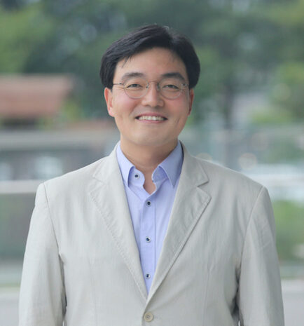
Prof. Dong Ki Yoon
KAISTPresentation title: Defects of liquid crystal and their phase transition.
Since beginning his career as a faculty member in KAIST about 9 years ago, Dong Ki Yoon has been actively engaged in research projects in the field of soft matters. Never content to rest on his laurels, Prof. Yoon has also continued integrating new, innovative concepts and thoughts in his research group. The research topics in his group can be categorized as following: (1) Nano- and Micro-Fabrication (2) Stimuli-responsive Supramolecules (3) Biopolymers for Patterning Application (4) LC Organic Electronics.
-
![]()
Bio
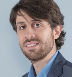
Prof. Lucio Isa
Associate Professor of Soft Materials and Interfaces, ETH ZurichPresentation title: Making micropatterns using capillary forces
Lucio Isa was born in Milan (Italy) in 1979. He obtained a Master’s degree (110/110 cum laude) in Nuclear Engineering from the Polytecnico di Milano (Italy) in 2004 and a PhD in Soft Matter Physics at the University of Edinburgh (UK) in 2008. After a short postdoctoral spell in Edinburgh, he moved to the Materials Department of ETH Zurich at the end of 2008 to work in the Laboratory for Surface Science and Technology, first as a Marie-Curie Fellow and then as a Swiss National Science Foundation (SNSF) Ambizione Fellow. In 2012 he was awarded a SNSF travel grant as visiting fellow at the Chemical Engineering Department of the University of California, Santa Barbara, USA. In September 2013 Lucio Isa became SNSF Assistant Professor, heading the Laboratory for Interfaces, Soft matter and Assembly in the Department of Materials at ETH Zurich. In April 2019, he was promoted to Associate Professor of Soft Materials and Interfaces.
Lucio Isa is a co-founder of Swiss Soft Days, an initiative aimed at creating a national network of scientists working in Soft Matter in Switzerland.
He lives in Zurich with his partner and two children.
Abstract
Liquid crystals (LCs) are materials composed of anisotropic building blocks with structural order and physical properties intermediate between isotropic fluids and crystalline solids.
In particular, on-demand, large anisotropic responses to external fields, such as electromagnetic and temperature fields, make LCs a prominent element in a broad range of optoelectronic devices, including displays and sensors. During the formation of specific LC structures, defects are inevitably generated, inhibiting device performance, and are therefore avoided. However, the possibility of controlling the nature and the spatial arrangement of LC defects holds the potential for a dramatic broadening of the applications of LCs, such as in micro-patterned surfaces, micro-lenses, vortex beam generators and particle manipulation systems.
Besides technological applications, LC defects have been long used as a tool for fundamental studies of topology in materials. Topological defects in LCs present striking similarities to those found in diverse systems at very different length scales, including superconductors, superfluids and soft ferromagnets, but with the essential advantage of being easily visualized in an optical microscope. In spite of their importance for both fundamental science and applications, to date there are only few studies that address the generation and modulation of LC defects at a phase transition, especially over macroscopic thin films.This proposal uniquely combines the expertise of the Korean partner in LC films and their applications with the expertise of the Swiss partner in micro and nanoparticle assembly to realize a comprehensive platform for large-scale LC films with engineered defects.
In particular, we propose to use sequential capillarity-assisted particle assembly (sCAPA), a technology developed by the Swiss partner, to realize arrays of micro and nanoparticles with full geometrical and compositional control. The particles will act as nucleation points for the defects; by choosing the size, material and spatial arrangements of the particles, we propose to create LC films with controlled defects. In this way, we expect to trigger interacting LC defects and examine their structural and optical properties with and without external temperature and electric fields, a topic that lies at the core of the expertise of the Korean partner.
By controlling the physical and chemical properties of the particles immersed in an anisotropic LC medium, we will furthermore investigate the analogy with quantum topological defects, whose strength and distortion fields cannot be easily experimentally controlled.
In detail, 1) the LC materials will be directly deposited on the patterned substrates to investigate the nucleation and growth of defects, depending on the geometrical and chemical properties of the particle arrays obtained by sCAPA.
2) Temperature gradients will be applied to study the competitive interaction between the topographic patterns and the thermal phase transition.
3) LC orientation will be externally controlled using electric fields to examine the elastic-dynamic behaviour of LC defects, which has so far received little attention.
4) Particle arrays will be deposited on patterned electrodes to realize new switchable optoelectronic films. Summarizing, this ambitious synergistic project will explore new aspects of defect engineering, an exciting field with broad implications for materials science, specifically applied to the case of LC films.
The outcome of the project will enable new technological applications in dynamic pattern generation and photonics, while furthering our fundamental understanding of topological defects in condensed matter.

